Memory organisation in cfx CASIO calculators
CPU of cfxs has very interesting features, something is very cool and usefull (variable data length up to 128 bit, LAR, conditional calls and returns), but it has also disadvantage, which limit all proram developers. I haven't found any documentation about the CPU, so all I write here is only result of my hacking.
Cfx has 16 bit addressing it menas, than without any additional feature the largest memory size (RAM+ROM together) would be 64KB - it's nothing for such device. So HW developers have added the possibility for bank switching. Cfx has 256 banks (HW maximum, not all used) and there are 3 special 8 bit registers to remember which bank use for memory operation (it menas which bank is for reading instructions - Code Segment, which for reading data - Data Segment and which for stack - Stack Segment). If you little know memory addressing in most used CPU i80x86 in real mode, you can think, that it's the same, but it's totaly different, please forgot all about i80x86 while reading this document. Every instruction (except one - far jump) working with memory takes only 16bit number (no matter if directly as a constant number or from the address register). In other words we can say, that memory is accessible as a matrix, we must specify a row (segment) and column (offset). Or we can say, that we are playing chess in this matrix, but we have only one tower.
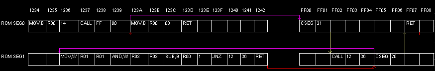
For data and stack accessing there is no problem, we can always set the segment register to the value we want (use instructions Dseg or Sseg) and then access data (specifying the 16bit offset). We can also to this for code segment, but such code would be very very unreadable and hard to write. You can imagine this like a chess game , where (in data +stack case) we can do many moves (how many we want) before we put the tower down. In code case (which is I want to write the rest of this text) we have only ONE move, so after putting tower down we must be sure there is usefull code to continue. CASIO programmers have solved this way, that they put routines which beholds together to one segment (to minimize segment-to-segment jumping) and for every target stored in another segment they created an access point (at the end of segment), where it is used instruction Cseg to go to target segment, here continues code (local call of target routine) and another Cseg to go back to our segment. See simple example (this code is NOT in any ROM, I created it only as a example):
start our routine at ROM Seg00:1234
move 0x14 to byte register R00 (loop count)
call access point at ROM Seg00:FF00
change segment to ROM Seg01 (ROM segments are mapped to segments 0x20 to 0x27)
call our routine at ROM Seg01:1236
run it's body - this is an example of "wait routine", it does R00 x a loop containing instructions with no result
return to our access point (we are at ROM Seg01:FF05)
change segment to ROM Seg01 (so we are at ROM Seg00:FF07)
return from access point to the routine, which started this all
do the rest of the first routine (we are at ROM Seg00:123A)
This example shows the CALL access point, cfx uses also JMP access points, they are one way only, so they are used in pairs (I used them in my ROM upgrade supporting ASM) or in singles (e.g. routines for errors have such access points).